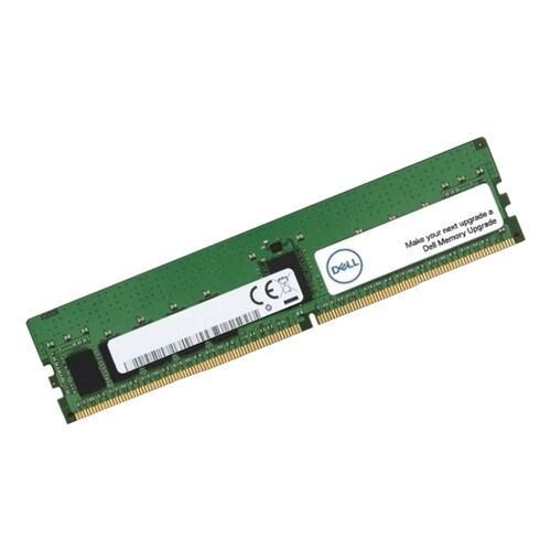
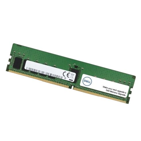
370-BBKG Dell 32GB PC5-38400 DDR5-4800B-E ECC SDRAM 288-Pin UDIMM Memory
- — Free Ground Shipping
- — Min. 6-month Replacement Warranty
- — Genuine/Authentic Products
- — Easy Return and Exchange
- — Different Payment Methods
- — Best Price
- — We Guarantee Price Matching
- — Tax-Exempt Facilities
- — 24/7 Live Chat, Phone Support
- — Visa, MasterCard, Discover, and Amex
- — JCB, Diners Club, UnionPay
- — PayPal, ACH/Bank Transfer (11% Off)
- — Apple Pay, Amazon Pay, Google Pay
- — Buy Now, Pay Later - Affirm, Afterpay
- — GOV/EDU/Institutions PO's Accepted
- — Invoices
- — Deliver Anywhere
- — Express Delivery in the USA and Worldwide
- — Ship to -APO -FPO
- — For USA - Free Ground Shipping
- — Worldwide - from $30
Dell 370-BBKG 32GB DDR5 Memory Module
The Dell 370-BBKG 32GB PC5-38400 DDR5-4800B-E ECC Unbuffered Dual Rank X8 SDRAM UDIMM is engineered for professionals who demand reliability, speed, and seamless multitasking. Designed with advanced DDR5 technology, this module ensures optimized performance for modern computing environments.
Manufacturer Information
- Brand Name: Dell
- Part Number: 370-BBKG
- Product Category: DDR5 SDRAM Memory Module
Technical Specifications
- Memory Capacity: 32GB
- Technology: DDR5 SDRAM
- Speed Rating: 4800 MT/s
- Standard: DDR5-4800 / PC5-38400
- Rank Configuration: Dual Rank X8
- Signal Type: Unbuffered
- Form Factor: UDIMM
- Pin Layout: 288-pin
Reliability
- Error Checking: ECC for dependable performance
- Optimized for professional-grade systems
Compatibility
Supported Dell
Alienware Series
- Alienware Aurora R13
- Alienware Aurora R15 (Intel)
OptiPlex Towers
- OptiPlex 7000 Tower
- OptiPlex XE4 Tower
Precision Workstations
- Precision 3660 Tower
- Precision 3660XE Tower
XPS Desktop
- XPS 8950
Dell 370-BBKG 32GB Memory Overview
The Dell 370-BBKG 32GB PC5-38400 DDR5-4800B-E ECC Unbuffered Dual Rank X8 SDRAM 288-Pin UDIMM memory module is a high-density, server- and workstation-focused DRAM solution engineered to deliver dependable performance, data integrity, and broad compatibility with modern DDR5-capable platforms. This category centers on premium, error-correcting code (ECC) unbuffered DDR5 memory modules that balance speed and stability for applications where uptime and correctness matter: virtualization hosts, database servers, scientific computing nodes, professional content creation workstations, and enterprise-class edge devices. The designation PC5-38400 and DDR5-4800 identifies the raw data throughput and JEDEC timing class, while the ECC Unbuffered Dual Rank X8 topology and 288-pin UDIMM form factor describe the module’s electrical layout and physical interface. Readers interested in memory upgrades, server builds, or fleet refresh projects find this category useful because it is tailored for systems that require ECC protection without the latency and cost of registered or load-reduced memory variants.
Key Technical
The model identifier encapsulates critical technical data: "32GB" indicates the module capacity, which is essential when planning memory capacity per socket and per node. "PC5-38400" denotes the theoretical peak bandwidth measured in megabytes per second per module — an estimate derived from the DDR5-4800 data rate multiplied by the bus width. "DDR5-4800B" signals adherence to the DDR5 standard with a 4800 MT/s baseline timing class; suffix letters (like the B) often indicate a specific timing bin or JEDEC profile. "E ECC" confirms the presence of single-bit error detection and correction capability integrated into the module, which is indispensable for many enterprise and professional deployments that enforce ECC at the BIOS or firmware level. "Unbuffered" sets this module apart from RDIMM and LRDIMM types by being directly driven by the memory controller without an interposing register or buffer, which typically reduces latency and simplifies compatibility with client and some server chipsets. "Dual Rank" reveals that memory chips are organized into two independent ranks, which can improve performance in certain memory controller implementations by increasing bank-level parallelism. "X8" defines the chip data width, impacting how many physical DRAM chips are placed on the module and influencing fault isolation and spare capacity. "SDRAM" establishes the synchronous DRAM family, and "288-Pin UDIMM" is the standard pin count and mechanical layout for many modern DDR5 unbuffered DIMMs.
Memory Architecture
Error-correcting code (ECC) is a core differentiator for this category. ECC memory modules detect and correct single-bit memory errors automatically, reducing the probability of silent data corruption and improving system resilience. The error-correcting circuitry may be implemented at the module level and leveraged by the platform’s memory controller and firmware. Dual rank modules contain two sets of DRAM chips that the memory controller can access independently; the controller may interleave accesses across ranks for improved throughput. The X8 chip configuration is commonly used to balance cost, density, and manufacturability: with eight-bit wide devices, a 32GB UDIMM will typically use multiple 8Gb or higher die-count chips arranged across both faces of the PCB. The chip organization interacts with platform requirements such as maximum rank count per channel and addressability limits defined by processor/motherboard vendors.
Form Factor
The 288-pin UDIMM layout is the mechanical standard for DDR5 unbuffered modules. The edge connector design and notch placement align with DDR5 slots on contemporary motherboards and server boards; electrical pinouts are assigned to ensure correct voltage rails, data strobes, and ECC lanes. While UDIMMs expose the memory controller to the full electrical load, modern server-grade memory controllers and motherboards are engineered to support multi-rank UDIMMs at standard JEDEC voltages. Integrators must consult motherboard documentation to confirm maximum supported rank counts and population rules per channel, particularly when populating all available memory slots for maximum capacity.
Performance
The PC5-38400 throughput figure represents a theoretical maximum bandwidth of roughly 38.4 GB/s per module when operating at DDR5-4800. Workloads that benefit from higher sustained bandwidth include large-scale data processing, memory-intensive scientific simulations, high-resolution video rendering, and in-memory databases. For transactional database workloads and latency-sensitive services, the latency characteristics of DDR5 compared to DDR4 can differ; DDR5 typically provides higher bandwidth at possibly higher raw latency numbers, but rank and channel optimizations often offset latency impacts in parallelized server tasks. The dual-rank layout can produce performance boosts in multi-threaded or multi-process environments by allowing the controller to alternate accesses and reduce bank conflicts, effectively increasing throughput under contention-heavy scenarios.
Use Cases
OEM-targeted DDR5 ECC UDIMMs such as the Dell 370-BBKG are often deployed in enterprise servers where ECC is required for regulatory or reliability reasons. Virtualized infrastructure benefits from the combination of capacity and integrity because guest VMs rely on correct memory contents. High-performance computing clusters and scientific instruments that run longstanding simulations or manage large in-memory arrays prefer ECC modules to avoid subtle bit rot that could invalidate results. Professional content creation workstations handling multi-gigabyte frames, complex 3D scenes, or multi-layer color grading also benefit from the extra capacity and error correction. Edge computing appliances processing real-time telemetry may use ECC UDIMMs to improve resilience in harsh operational conditions where hardware replacement is costly or slow. In each scenario, the ability to mix capacity and maintain consistent error correction simplifies provisioning, backup, and SLAs for mission-critical applications.
Compatibility
Compatibility is a critical element for buyers of high-density ECC UDIMMs. Server and workstation OEMs publish memory compatibility lists or validated DIMM matrices that indicate supported capacities, ranks, and speed profiles for each CPU and motherboard revision. While JEDEC compliance improves the probability that a module will function, platform firmware quirks, preferred voltage margins, and channel-loading limitations can affect stability or performance. Administrators should consult vendor technical documentation, QVL (Qualified Vendor List) tables, and BIOS release notes to ensure a chosen module will operate at its rated speed and with ECC enabled. Mixing DDR5 modules of different densities, ranks, or JEDEC timing bins can work in many cases but may force the memory subsystem into the lowest common denominator for speed or timings or require manual configuration in BIOS.
Thermal
DDR5 introduces on-die power management features and improved power efficiency compared to earlier generations, yet higher-speed JEDEC bins like DDR5-4800 and higher-capacity modules draw more power under sustained activity. ECC UDIMMs with dense die counts can exhibit elevated operating temperatures in heavily populated memory channels. Server chassis designs account for this by directing airflow across DIMM banks and using motherboard thermal sensors to prevent adverse effects. Module vendors and system integrators recommend following airflow guidelines and avoiding obstructing memory cooling paths. Some heat spreader implementations exist for high-performance desktop or workstation memory, but OEM server UDIMMs often rely on chassis-level airflow and optimized board power delivery rather than tall heat sinks. Power delivery stability is critical because voltage fluctuations can cause memory errors; robust power regulation on the motherboard and proper PSU sizing for overall system load are essential when populating multiple 32GB DDR5 modules across several channels.
Comparisons
Understanding the relative trade-offs between ECC UDIMM, RDIMM (Registered DIMM), and LRDIMM (Load-Reduced DIMM) helps systems architects align memory selection with performance and capacity targets. ECC UDIMMs offer lower latency than registered memory because there is no address/command register between the controller and DRAM chips, which can be beneficial in certain workstation and entry-level server scenarios. RDIMMs insert a register to buffer control signals, reducing electrical load and allowing higher DIMM counts per channel with a small latency penalty, which suits large-capacity enterprise servers. LRDIMMs further reduce electrical load by buffering both address/control and data, enabling very high densities per channel but introducing additional complexity and slightly greater latency.


