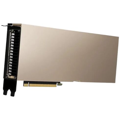
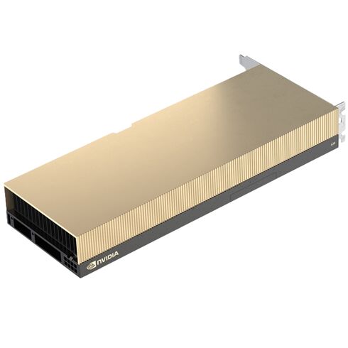
900-21001-0100-030 Nvidia A100 40GB HBM2 PCI-E 6912 Cuda Cores GPU
- — Free Ground Shipping
- — Min. 6-month Replacement Warranty
- — Genuine/Authentic Products
- — Easy Return and Exchange
- — Different Payment Methods
- — Best Price
- — We Guarantee Price Matching
- — Tax-Exempt Facilities
- — 24/7 Live Chat, Phone Support
- — Visa, MasterCard, Discover, and Amex
- — JCB, Diners Club, UnionPay
- — PayPal, ACH/Bank Transfer (11% Off)
- — Apple Pay, Amazon Pay, Google Pay
- — Buy Now, Pay Later - Affirm, Afterpay
- — GOV/EDU/Institutions PO's Accepted
- — Invoices
- — Deliver Anywhere
- — Express Delivery in the USA and Worldwide
- — Ship to -APO -FPO
- — For USA - Free Ground Shipping
- — Worldwide - from $30
Brand Information
- Manufacturer: Nvidia
- Model Identifier: 900-21001-0100-030
- Device Category: High-Performance Graphics Processing Unit
Core Architecture
Processing Unit
- Chipset Name: GA100
- Microarchitecture: Ampere-based design
- Fabrication Node: 7-nanometer process technology
Frequency Metrics
- Base GPU Frequency: 1095 MHz
- Maximum Boost Rate: 1410 MHz
- Memory Speed: 1215 MHz
Memory Configuration
Memory Specifications
- Capacity: 40 GB
- Type: HBM2e (High Bandwidth Memory)
- Bus Interface: 5120-bit memory bus
- Data Transfer Rate: Up to 1,555 GB/s
Power and Connectivity
Power Requirements
- Thermal Design Power (TDP): 250 Watts
- Power Connector: Single 8-pin CPU auxiliary input
Output Configuration
- Display Outputs: None available
- Slot Form Factor: Integrated Graphics Profile (IGP)
Rendering Capabilities
Shader and Texture Units
- CUDA Cores: 6912 parallel processors
- Texture Mapping Units (TMUs): 432
- Render Output Units (ROPs): 160
- Streaming Multiprocessors (SMs): 108
- Tensor Core Count: 432 specialized cores
Computational Throughput
Floating Point Performance
- FP64 (Double Precision): 9.7 TFLOPS
- FP64 via Tensor Cores: 19.5 TFLOPS
- FP32 (Single Precision): 19.5 TFLOPS
Advanced Tensor Operations
- TF32 (Tensor Float 32): 156 TFLOPS (standard) / 312 TFLOPS (sparse)
- BFloat16 Tensor Core: 312 TFLOPS (standard) / 624 TFLOPS (sparse)
- FP16 Tensor Core: 312 TFLOPS (standard) / 624 TFLOPS (sparse)
- INT8 Tensor Core: 624 TOPS (standard) / 1248 TOPS (sparse)
Nvidia 900-21001-0100-030 A100 40GB GPU Overview
The Nvidia 900-21001-0100-030 A100 40GB HBM2 PCI-E 4.0 x16 is a purpose-built data center accelerator designed around Nvidia's Ampere GA100 GPU. This SKU delivers a balanced blend of large, high-bandwidth memory, massive parallel compute resources, and platform-level features tailored for AI training, inference at scale, scientific simulation and high performance computing (HPC). At the silicon level the A100 integrates thousands of CUDA cores and hundreds of third-generation Tensor Cores that together accelerate dense linear algebra, mixed precision math, and tensor operations used across neural network training and inference pipelines. The PCIe form factor enables straightforward integration into a wide range of enterprise and server-class motherboards while keeping density and deployment flexibility high for rack servers and workstation nodes.
Compute Resources
The A100 40GB variant implements a GA100 configuration that includes 6,912 CUDA cores distributed across 108 streaming multiprocessors (SMs), together with an array of third-generation Tensor Cores optimized for matrix multiply and accumulation workloads. This hardware composition provides exceptional FP32 and mixed-precision throughput for modern deep learning frameworks while also offering strong FP64 and INT capabilities for traditional HPC and scientific computing tasks. Developers targeting maximum throughput for training large transformer models or scaling multi-node distributed training will see the benefits of the dense CUDA and Tensor Core counts when codepaths are written to exploit Tensor Core mixed-precision primitives.
Memory
Memory capacity and bandwidth are fundamental to large model training and memory-bound HPC kernels. The 900-21001-0100-030 A100 ships with 40GB of high-bandwidth memory (HBM2/HBM2e depending on manufacturing and subvariant) organized on a wide 5,120-bit memory bus. The resulting aggregate memory bandwidth for the 40GB PCIe card is in excess of 1.5 TB/s, enabling sustained data delivery to the compute fabric and reducing stalls for large tensors and batched workloads. This high memory throughput is particularly valuable for sparse matrix operations, distributed data loading, and multi-tensor kernels that push memory traffic more than raw arithmetic. When architecting a system around the A100, pay close attention to I/O and host memory paths to avoid creating bottlenecks that would prevent the GPU from saturating its HBM bandwidth.
Form Factor
The PCI-Express variant of the A100 is a dual-slot passive cooled card intended for systems with directed chassis airflow. The PCIe Gen4 x16 interface provides the necessary host connectivity while the passive heat sink design places the responsibility for cooling on the system-level airflow and thermal design. Thermal Design Power (TDP) for the PCIe 40GB A100 typically sits in the mid-hundreds of watts range depending on the exact OEM configuration and firmware power profiles, and typical PCIe card configurations for server vendors list a TDP around 250W for standard PCIe implementations. System integrators must verify adequate power headroom, proper airflow routing, and BIOS/firmware settings to make sure the card operates inside its thermal envelope under full sustained load.
Key Platform Features
The A100 is feature rich for modern data center workloads. Multi-Instance GPU (MIG) enables partitioning of the physical GPU into multiple secure, isolated GPU instances to better match mixed workload environments and improve utilization across diverse job sizes. Built-in support for unified virtual memory and page migration engines simplifies programming models for large datasets by allowing the GPU and CPU to more seamlessly share memory spaces. For multi-GPU deployments, Nvidia’s communication libraries and stack components such as NCCL provide high-efficiency collective communications and topology-aware tensor reduction primitives essential for scaling training across nodes with RDMA networking. These platform features collectively reduce time-to-solution for AI experiments and streamline deployment for production inference clusters.
Software
The A100 is supported by the full Nvidia software stack including CUDA, cuBLAS, cuDNN, TensorRT, NVSwitch-aware libraries for supported variants, and Nvidia Data Center GPU Manager (DCGM) for telemetry, health checks and monitoring. Mainstream machine learning frameworks like PyTorch and TensorFlow provide optimized kernels and automatic mixed precision paths that exploit the A100’s Tensor Cores automatically when compiled against suitable CUDA and cuDNN versions. For inference deployments, TensorRT and ONNX-based pipelines can further compress and optimize models to make inference cost effective, while graph optimizations lower latency and increase throughput per watt. The combination of hardware and software makes the A100 a practical choice for teams looking to accelerate from prototype models to production at scale without significant code rewrites.
Workloads
The A100 excels in workloads where dense matrix math, tensor operations, and large model parameter storage dominate compute time. Training of large transformer models, BERT-scale NLP models, wide deep learning recommender systems, and large-batch image classification all see material speedups from the A100’s tensor throughput and memory bandwidth. Scientific computing workloads that rely on mixed precision or that can be refactored to exploit tensor acceleration—such as computational chemistry, molecular dynamics, finite element solvers and climate modeling—also benefit. For inference, batched or pipelined low-latency services can be dramatically densified on A100s when paired with optimized runtime stacks and model quantization. Because the PCIe variant is easier to deploy into standard servers, organizations with existing rack infrastructure can adopt the A100 without the platform redesign sometimes required by SXM form-factor cards.
Multi-GPU
When building multi-GPU clusters, network topology and interconnect bandwidth become as important as per-GPU peak FLOPS. The A100 PCIe cards can be used in multi-node training through high bandwidth networking fabrics such as RoCE or InfiniBand combined with NCCL to provide efficient all-reduce and gradient synchronization. For intra-node dense interconnects and ultra-low latency, SXM modules and NVLink/NVSwitch provide higher inter-GPU bandwidth than PCIe, but PCIe cards remain viable for many distributed training topologies where the network is the dominant scaling factor. MIG can be used to subdivide GPUs to serve many smaller concurrent jobs, improving overall utilization in shared clusters and offering a flexible way to match GPU allocation to workload requirements.
Performance
Achieving the best performance on an A100 involves algorithmic and engineering choices across precision, memory layout and kernel selection. Using mixed precision (for example FP16 with loss scaling or Nvidia’s TF32 on supported kernels) unlocks Tensor Core performance while retaining model convergence behavior. Efficient memory tiling, fused kernel use, and minimizing host–device transfers reduce stalls and allow the GPU to run near its arithmetic roofline. Profiling with Nvidia Nsight and analysis with DCGM identify hot paths and bottlenecks so engineers can focus on the kernels that yield the largest improvements. Choosing the right batch size to maximize utilization without overflowing HBM is also a critical step in tuning.
Compatibility
Integrating A100 PCIe cards into an existing server fleet requires careful attention to mechanical fit, power delivery and airflow. Because the PCIe A100 is a dual-slot passive card, chassis designs must provide consistent front-to-back airflow and sufficient fan capacity. Server BIOS settings such as PCIe speed negotiation, SR-IOV enablement for virtualization, and UEFI firmware updates can also influence behavior under load. On the software side, driver versions, CUDA toolkit compatibility and OS kernel settings for PCIe and hugepages must be coordinated to ensure stable, high-performing deployments. Vendors who ship the 900-21001-0100-030 SKU often provide system integration notes and validated configurations to reduce integration time and risk.
Comparisons
The Ampere A100 represents a generational leap over previous data center GPUs by combining larger HBM capacities, a redesigned SM/Tensor Core architecture and improved software ecosystem maturity. Compared with earlier Volta and Turing generations, the A100 delivers much higher tensor throughput and more flexible precision modes, enabling both higher peak performance and better sustained results on modern AI workloads. For procurement decisions, consider whether the 40GB memory is sufficient for your target models or if the 80GB A100 variants or SXM alternatives are needed for very large models. The A100’s performance and programmability mean it remains relevant for multiple generations of software, but careful planning around driver and CUDA toolkit updates is necessary to maintain long-term compatibility.
Use Cases
Across industries the A100 has been used to accelerate large language model training, real-time recommendation systems for e-commerce, genomics analysis pipelines with accelerated sequence alignment, and complex fluid dynamics simulations in engineering. Successful projects typically combine algorithmic changes to exploit mixed precision, efficient data pipelines to ensure GPUs remain fed, and orchestration layers that balance experiment throughput with business priorities. The A100’s versatility allows organizations to run a research experiment in the morning and scale a production inference service by evening, provided that the deployment practices around containerization, monitoring and rollback are in place.


